I recently wrote an application note on using AFM to characterize two-dimensional materials for AFMWorkshop. The full article can be found here. What follows is a brief extract.
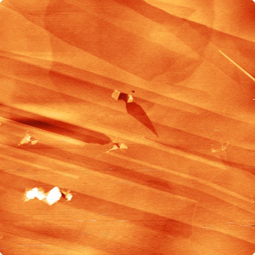
Two dimensional materials are currently under development with potential to gain enormous importance in electronics, sensing, optics and other areas. Such materials, despite facile production methods in many cases, can display radically different properties compared to 3D or bulk materials. These new and enhanced properties come about due to nanoscale confinement effects, meaning they are generally accessible only when a material is limited to one, or at most to a few atomic layers. For this reason, research and development in 2D material and 2D materials-based devices relies crucially on the ability to characterise such materials at the nanoscale, including the observation of atomic steps. Atomic Force Microscopes are ideally suited for creating 3-D images and measurements on 2-D materials. This is because AFMs have extreme contrast on flat samples and can magnify surface heights by factors of millions to billions. AFM is unique in its ability to measure sample heights with resolution in excess of 0.1 nm. This explains why AFM has become a key tool in the arsenal of researchers studying 2D materials - for example, see the two images of layered materials below.
 |
 |
Figure 1a: Three dimensional color scaled image of SiC. The steps on this sample are 750 picometers.
Figure 1b: Colourscale image of HOPG, showing atomic steps.
Besides illustrating the power of an AFM, these types of samples serve as calibration samples for microscopes used for imaging 2-D materials.
Graphene is an extraordinary new two-dimensional material, consisting of single atomic layers of sp2 carbon. Although graphene is a single atom thick sheet, it is not typically found to be perfectly flat. Indeed, some nanometre scale corrugations, are commonly observed and may increase the stability of the 2D lattice. Despite its great strength, graphene is also a highly flexible material, and typically takes on the form of the underlying substrate. So, for example, on Si/SiO2 wafers, graphene can exhibit a considerable roughness due to the underlying substrate. Thus, a considerable texture, dependent on the SiO2 structure at the wafer surface, can be seen in the CVD graphene flakes shown in the left image in figure 2 below.

Figure 2. Examples of AFM images of CVD graphene deposited on Si/SiO2 wafers. Left: Single-layer graphene on a silicon wafer. In this example, the effect of the underlying texture on the graphene sheet is clearly seen. Right: Multilayer graphene of a silicon wafer. Arrows highlight some wrinkle-like defects, typical of CVD graphene.
To read more about AFM applications to two-dimensional materials, read the full application note here.