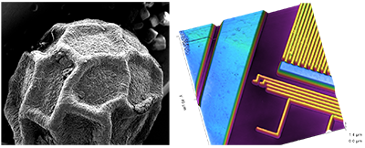
This is the first of a series of answers written to compare AFM to other techniques. SEM (scanning electron microscopy) is a high resolution surface microsocpy technique, so it's very comparable with AFM. In some cases the two methods can give similar results, but in many they vary greatly in terms of the type of results obtained, the ease of use, and in many other ways.
How does AFM (atomic force microscopy) compare to SEM (scanning electron microscopy)?
In this article, the performance of SEMS and AFMs are comapred. The article starts with an introduction to SEM. For an introduction to or refresher on, AFM, check here.
Scanning Electron Microscopy
A scanning electron microscope is a type of electron microscope. Electron microscopes (EMs) use an accelerated beam of electrons, instead of light, to probe a sample. The SEM was the second type of EM to be invented after the transmission electron microscope (TEM). SEM was invented in the 1930s but they first became commercially available in the 1960s. SEMs took a while to be popular compared to TEMs, as they require more complex electronics.
The SEM uses an electron source, which is often a fine heated wire. Electrons are accelerated away from the wire with a nearby anode at a high positive potential. Electron lenses are used to focus the spreading electrons into a beam, and eventually focus this beam into a small spot on the sample surface. A set of scanning coils are used to raster this spot across the sample surface in an area chosen by the operator. When electrons strike the sample, some electrons bounce back (they are "backscattered"), and some electrons are knocked out of the orbits of sample atoms. The SEM has one or more detectors which detect these emitted electrons. On a computer screen, the intensity of the detected electrons is plotted versus the location of the beam on the sample, to form the image. The intensity of electrons emitted depends on the sample topography, and also it's materials, with more electron -dense elements (i.e larger atomic number) emitting more electrons. On modern SEM instruments there are often multiple detectors, allowing the operator to record signals more close to topography or composition. Many SEMS also include x-ray detectors, allowing a technique called energy dispersive x-ray spectroscopy (EDX). This allows the EM to act as a spectrometer and detect which elements are present in the sample.

Example images from an SEM (left, shwoing black pepper grain), and an AFM (right, showing interated circuit interconnects)
Resolution
Since AFM and SEM work in very different ways it’s not simple to compare their resolution. In simple terms, the SEM’s resolution is controlled by the spot size it uses. The smaller the spot the SEM can focus the electron beam to, the higher it’s resolution can be. The size of the spot is controlled by the type of electron source used and the quality of the electron optics. This means that to achieve higher resolution, advanced SEMS tend to be larger and more expensive. However, the nature of the sample can often affect the achievable resolution in the SEM. This is because SEMS use a highly energetic electron beam as a probe. When the electron beam hits the sample, electrons will penetrate a certain distance into the sample and be scattered by interaction with the sample, before being emitted. Therefore, if the electron beam is focussed to a very small spot, the actual interaction area may be larger than this spot, decreasing resolution. The size of this interaction area depends on how electron-dense the sample is. So, resolution on some samples will be better than on others. SEM manufacturers often claim resolution values around 1.5 nm for very advanced microscopes. But this resolution can only be demonstrated on particular samples. So SEM resolution would vary between 1.5 to 5 nm for a high performance SEM.
The resolution of most AFMs are limited by probe size and noise. The probe size limits the lateral (X-Y resolution), just as it does in SEM. However, the probe in AFM does not penetrate the sample, so the smaller the probe, the higher the lateral resolution. For AFM modes involving probe-sample contact in air, there is a practical limit to how small the probe can be, and not become contaminated or broaden by wear during scanning. Therefore it is hard to achieve lateral resolution higher than 1-3 nm in AFM in air. Scanning in liquid, controlled atmosphere or vacuum can overcome these problems, and very high resolution can be achieved. The highest resolution achieved in this way is on the order of 200 pm, or 0.2 nm. On the other hand, in the z direction (sample height), the achievable resolution is limited by instrument noise. In air, the noise in many systems is limited by thermal noise in the cantilever, and 100 pm can be achieved. This would be improved in vacuum systems as well.
Overall, the AFM and SEM can achieve similar resolutions under common imaging conditions, but AFM’s ultimate resolution is greater than that of SEM.
Sample types
Both AFM and SEM can be used with a fairly wide range of samples. SEM is fairly restrictive in that samples must be conductive and also vacuum-resistant. Some SEMS are capable of measuring samples in a low pressure atmosphere, and can cope with some resistivity on the samples, but generally under these conditions limited resolution can be achieved. However, there are well known procedures which can be used to make almost any sample resistant to vacuum and to the electron beam, notably chemical fixation followed by dehydration, and coating with a thin metal film. AFM, on the other hand, can cope with any sample, be it metal or insulator, and even samples containing small amounts of water. If fully hydrated, samples can be imaged in a liquid cell.
SEM is suitable for imaging very large samples, with extreme roughness, which is difficult for AFM. On the other hand, AFM can give very strong contrast on extremely smooth samples, which migth appear featurelss in the SEM.
Due to the issues described above, sample preparation can be complex for SEM, compared to AFM, especially for biological samples. On the other hand, metallic samples require almost no preparation. Sample preparation for AFM is often very simple for almost all samples.

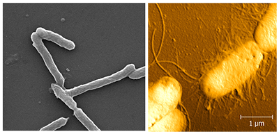
Images of biological samples from SEM (left) and AFM (right). Both images show E. coli bacteria. The samples for SEM must be carefully fixed and dried in sequential solutions before imaging. AFM images can be obtained by simple air-drying.
Information
The kind of information provided by the two techniques can be very different. SEM usually shows images that give an idea of the shape and dimension of sample features. Other detectors produce contrast based on atomic number. One of the most useful techniques is EDX, which can measure the types of elements present, and even give concentrations of different elements. With EDX mapping, the distribution of different elements over an area can be displayed.
The most common AFM mode mode is also topographic, and it gives fully three dimensional data, so both X, Y and Z data can be obtained from any part of the sample. To do this in SEM, a cross-section must be produced, or the sample tilted, and imaged from the side. AFM can also provide mechanical characterisation of the sample, such as measuring hardness, viscoelastic properties, and friction measurements. Advanced techniques on the AFM can also measure other properties like magnetic fields, electrical properties, or the force of molecular interactions.
Cost
SEMs are generally considerably more expensive than AFM instruments to purchase. There are some compact SEM instruments that cost around 100,000 USD, but these are often capable of only low resolutions, and limited in features. An advanced SEM could easily cost 500,000 USD.
On the other hand, AFM instruments, such as those from AFMWorkshop, can produce extremely high resolution images, at a very low instrument cost (<50,000 USD). More advanced instruments, with many different modes can cost 200,000 USD.
AFM does come with a consumables cost; AFM probes are considered a consumable item, as they need to be replaced regularly. The consumable cost for many SEMs is only electricity, some instruments cna use liquid nitrogen to cool the EDX detector.
Speed of Imaging
SEMs generally collect data much faster than AFMs. A low quality SEM image can be acquired in a few seconds, and a high quality one in under a minute. AFM images generally take a few minutes to acquire. New Fast-scanning AFMs are beginning to appear which can collect images in a few seconds or less.
All information, text and images copyright 2021 Peter Eaton