
|
My name is Peter Eaton, and I have been working with Atomic Force Microscopy for more than 20 years. I am currently an Instrument Scientist at The Bridge, in the University of Lincoln, UK. I am the co-author (with Paul West of AFMWorkshop) of the book Atomic Force Microscopy, published in 2010 by Oxford University Press. I have collaborated with researchers in the UK, France, Spain, Brazil, Argentina, Portugal, the USA and Germany in AFM. I have taught AFM around the globe, and am the coordinator of the well-known Porto AFM Training Workshop (running from 2011 onwards). In addition to development of research and education in Atomic Force Microscopy, my interests include: Antimicrobial peptides derived from amphibians
A complete list of my research papers can be found along with my academic CV here. I have co-authored more than 90 scientific works. I am happy to collaborate scientifically in interesting projects or carry out scientific consultancy in the field of atomic force microscopy. |
 |
- Details
- Hits: 33003
This is the first of a series of answers written to compare AFM to other techniques. SEM (scanning electron microscopy) is a high resolution surface microsocpy technique, so it's very comparable with AFM. In some cases the two methods can give similar results, but in many they vary greatly in terms of the type of results obtained, the ease of use, and in many other ways.
How does AFM (atomic force microscopy) compare to SEM (scanning electron microscopy)?
In this article, the performance of SEMS and AFMs are comapred. The article starts with an introduction to SEM. For an introduction to or refresher on, AFM, check here.
Scanning Electron Microscopy
A scanning electron microscope is a type of electron microscope. Electron microscopes (EMs) use an accelerated beam of electrons, instead of light, to probe a sample. The SEM was the second type of EM to be invented after the transmission electron microscope (TEM). SEM was invented in the 1930s but they first became commercially available in the 1960s. SEMs took a while to be popular compared to TEMs, as they require more complex electronics.
The SEM uses an electron source, which is often a fine heated wire. Electrons are accelerated away from the wire with a nearby anode at a high positive potential. Electron lenses are used to focus the spreading electrons into a beam, and eventually focus this beam into a small spot on the sample surface. A set of scanning coils are used to raster this spot across the sample surface in an area chosen by the operator. When electrons strike the sample, some electrons bounce back (they are "backscattered"), and some electrons are knocked out of the orbits of sample atoms. The SEM has one or more detectors which detect these emitted electrons. On a computer screen, the intensity of the detected electrons is plotted versus the location of the beam on the sample, to form the image. The intensity of electrons emitted depends on the sample topography, and also it's materials, with more electron -dense elements (i.e larger atomic number) emitting more electrons. On modern SEM instruments there are often multiple detectors, allowing the operator to record signals more close to topography or composition. Many SEMS also include x-ray detectors, allowing a technique called energy dispersive x-ray spectroscopy (EDX). This allows the EM to act as a spectrometer and detect which elements are present in the sample.

Example images from an SEM (left, shwoing black pepper grain), and an AFM (right, showing interated circuit interconnects)
Resolution
Since AFM and SEM work in very different ways it’s not simple to compare their resolution. In simple terms, the SEM’s resolution is controlled by the spot size it uses. The smaller the spot the SEM can focus the electron beam to, the higher it’s resolution can be. The size of the spot is controlled by the type of electron source used and the quality of the electron optics. This means that to achieve higher resolution, advanced SEMS tend to be larger and more expensive. However, the nature of the sample can often affect the achievable resolution in the SEM. This is because SEMS use a highly energetic electron beam as a probe. When the electron beam hits the sample, electrons will penetrate a certain distance into the sample and be scattered by interaction with the sample, before being emitted. Therefore, if the electron beam is focussed to a very small spot, the actual interaction area may be larger than this spot, decreasing resolution. The size of this interaction area depends on how electron-dense the sample is. So, resolution on some samples will be better than on others. SEM manufacturers often claim resolution values around 1.5 nm for very advanced microscopes. But this resolution can only be demonstrated on particular samples. So SEM resolution would vary between 1.5 to 5 nm for a high performance SEM.
The resolution of most AFMs are limited by probe size and noise. The probe size limits the lateral (X-Y resolution), just as it does in SEM. However, the probe in AFM does not penetrate the sample, so the smaller the probe, the higher the lateral resolution. For AFM modes involving probe-sample contact in air, there is a practical limit to how small the probe can be, and not become contaminated or broaden by wear during scanning. Therefore it is hard to achieve lateral resolution higher than 1-3 nm in AFM in air. Scanning in liquid, controlled atmosphere or vacuum can overcome these problems, and very high resolution can be achieved. The highest resolution achieved in this way is on the order of 200 pm, or 0.2 nm. On the other hand, in the z direction (sample height), the achievable resolution is limited by instrument noise. In air, the noise in many systems is limited by thermal noise in the cantilever, and 100 pm can be achieved. This would be improved in vacuum systems as well.
Overall, the AFM and SEM can achieve similar resolutions under common imaging conditions, but AFM’s ultimate resolution is greater than that of SEM.
Sample types
Both AFM and SEM can be used with a fairly wide range of samples. SEM is fairly restrictive in that samples must be conductive and also vacuum-resistant. Some SEMS are capable of measuring samples in a low pressure atmosphere, and can cope with some resistivity on the samples, but generally under these conditions limited resolution can be achieved. However, there are well known procedures which can be used to make almost any sample resistant to vacuum and to the electron beam, notably chemical fixation followed by dehydration, and coating with a thin metal film. AFM, on the other hand, can cope with any sample, be it metal or insulator, and even samples containing small amounts of water. If fully hydrated, samples can be imaged in a liquid cell.
SEM is suitable for imaging very large samples, with extreme roughness, which is difficult for AFM. On the other hand, AFM can give very strong contrast on extremely smooth samples, which migth appear featurelss in the SEM.
Due to the issues described above, sample preparation can be complex for SEM, compared to AFM, especially for biological samples. On the other hand, metallic samples require almost no preparation. Sample preparation for AFM is often very simple for almost all samples.

Images of biological samples from SEM (left) and AFM (right). Both images show E. coli bacteria. The samples for SEM must be carefully fixed and dried in sequential solutions before imaging. AFM images can be obtained by simple air-drying.
Information
The kind of information provided by the two techniques can be very different. SEM usually shows images that give an idea of the shape and dimension of sample features. Other detectors produce contrast based on atomic number. One of the most useful techniques is EDX, which can measure the types of elements present, and even give concentrations of different elements. With EDX mapping, the distribution of different elements over an area can be displayed.
The most common AFM mode mode is also topographic, and it gives fully three dimensional data, so both X, Y and Z data can be obtained from any part of the sample. To do this in SEM, a cross-section must be produced, or the sample tilted, and imaged from the side. AFM can also provide mechanical characterisation of the sample, such as measuring hardness, viscoelastic properties, and friction measurements. Advanced techniques on the AFM can also measure other properties like magnetic fields, electrical properties, or the force of molecular interactions.
Cost
SEMs are generally considerably more expensive than AFM instruments to purchase. There are some compact SEM instruments that cost around 100,000 USD, but these are often capable of only low resolutions, and limited in features. An advanced SEM could easily cost 500,000 USD.
On the other hand, AFM instruments, such as those from AFMWorkshop, can produce extremely high resolution images, at a very low instrument cost (<50,000 USD). More advanced instruments, with many different modes can cost 200,000 USD.
AFM does come with a consumables cost; AFM probes are considered a consumable item, as they need to be replaced regularly. The consumable cost for many SEMs is only electricity, some instruments cna use liquid nitrogen to cool the EDX detector.
Speed of Imaging
SEMs generally collect data much faster than AFMs. A low quality SEM image can be acquired in a few seconds, and a high quality one in under a minute. AFM images generally take a few minutes to acquire. New Fast-scanning AFMs are beginning to appear which can collect images in a few seconds or less.
All information, text and images copyright 2021 Peter Eaton
- Details
- Hits: 24255
During July 2020, the AFMBiomed summer school series was supposed to take place in Marseille, France. Due to CoVID travel restrictions, the course took place online. However, since, there was no travel involved, and because the organizers kindly decided to make signup free, the school, had a record number of participants. At times 300 people were online, which is amazing for a specialized course like this, and showed just how many people around the world want to learn about and improve their AFM!

The lecturers were really great, and despite working in this field for 20 years, even I learned some things! Since I thought the material was so good, I am including links to the archived lectures below. The "tutorial" lectures were particularly good. Note that although the overall topic was "Biomedical Science", there are techniques here that could be useful for any AFM user.
This link contains the lectures in .pdf format: https://amubox.univ-amu.fr/s/rtXJTnXZmsBc6XQ
Here You can find many of the lectures posted as videos on this site: https://zenodo.org/communities/afmbiomed?page=1&size=20
I highlight here some of the video tutorials that I found really useful:
- Nicolas Buzhinsky; - Mica surface preparation - especially for liquid applications: https://zenodo.org/record/3957408#.X1n5RHlKiUk
- Fidan Sumbul, Claire Valotteau and Felix Rico; - Cantilever and coverslip cleaning and surface coating methods and tips: https://zenodo.org/record/4017765#.X1n43HlKiUk
- Jean Luc Pellequer and Felix Rico; - Calibration of AFM cantilevers and optical response for force spectroscopy: https://zenodo.org/record/4005520#.X1n5r3lKiUk
Please note that these video are published with a DOI record, therefore, it would be helpful to the authors if you cite them. I found this online class really great, and hope it returns!
- Details
- Hits: 8785
TT-AFM noise floor measurement
This procedure can also be applied to other AFMWorkshop instruments. For tip-scanning instruments such as the LS-AFM or NP-AFM, the results will show larger noise floors, while for the HR-AFM, extremely lownoise floors can be achieved. The TT2-AFM is practically identical to the first-gen TT-AFM in terms of noise floor.
Procedure
1. Place a clean silicon calibration sample on the scanner.
2. Place a new probe in the instrument.
3. For this comparison, use vibrating mode. Setup the optical alignment and Tune Frequency as normal.
4. Select parameters to test are listed below. note that for a fair comparison, you can use parameters relevant to your typical measurements. The parameters described here, will give you an “ideal” value, i.e the best result possible.
|
Suggested parameters |
|
|
Parameter |
Suggested value |
|
X Gain % |
0 |
|
Y Gain % |
0 |
|
XY HV Gain |
Initially 1 (note it should be 0 for the actual measurement) |
|
Z HV Gain |
3* |
|
Image Add |
Off |
|
Z Feedback values |
Values you typically use, for example Gain 1.5, Proportional 150, Integral 1500 |
|
Lines |
128 |
|
speed |
1 Hz |
|
Left Image |
Z_DRIVE |
|
Samples/Pixel |
25 |
* Z HV Gain is the most important parameter controlling the noise, if the measurement is being made under low-noise conditions. Lower values will give lower values. However, lower values also decrease the overall z range of the scanner, making approaching problematic in non-ideal conditions. For a 17 microns scanner, decreasing this value may reduce noise further. Below a value of 3, it's unlikely to improve noise much.
Note that you can use any different parameters you like for this, and they can and will alter the results that you get. Also, the instrument should be properly calibrated in z to allow comparison with any other values. Be aware that tip approach with Z HV gain at 5 will be slow, and some post-approach adjustments might be necessary.(i.e Jog Down).
5. Go into feedback, and scan an image of a small area of the surface (XY HV Gain of 1). The image should be clean, with very few features visible. Ensure you end the scan with the probe on a flat part of the sample.
6. Withdraw probe.
7. Set scan size to 0, by using XY HV Gain = 0.
8. Approach surface again.
NOTE: It is important that you go into feedback on the surface in the same way as you did when you scanned an image. If you go into false feedback (probe almost but not quite, on the surface), you will not make a valid noise floor measurement.
9. Scan another image. No sample features should appear, as scan size is zero. The image may look something like the image below, or have some regular patterns in it.
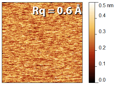
10. Save the file, and open the Left image - z piezo drive file (height image) in gwyddion.
11. Apply a 1st order polynomial levelling (fit linear).
12. Use “Statistical Quantities” and record the RMS average roughness (Sq). This is the noise floor
You should get a value of <1 angstrom (Gwyddion reports this in picometers, typically, so you expect to see a value of <100 pm).
If you do not get a satisfactory value, try removing sources of external vibration (other machinery, acoustic noise, unnecessary cables) from the instrument. Ensure probe and sample are grounded. Ensure that the vibration isolation system is setup properly.
Typical values found in a TT-AFM in an acoustically shielding box, with bungee-cord type isolation, would be 0.3 to 0.6 angstrom, 300 to 600 pm. Significant external noise will increase this.
You should be able to achieve at least the value specified by AFM workshop on the instrument specification sheet which was delivered with your instrument.
For an AFMWorkshop HR-AFM, achievable nosie floors can be less than 100 pm.
All materials on this website are copyright 2010-2018 Peter Eaton.
- Details
- Hits: 32263
I recently wrote an application note on using AFM to characterize two-dimensional materials for AFMWorkshop. The full article can be found here. What follows is a brief extract.
Two dimensional materials are currently under development with potential to gain enormous importance in electronics, sensing, optics and other areas. Such materials, despite facile production methods in many cases, can display radically different properties compared to 3D or bulk materials. These new and enhanced properties come about due to nanoscale confinement effects, meaning they are generally accessible only when a material is limited to one, or at most to a few atomic layers. For this reason, research and development in 2D material and 2D materials-based devices relies crucially on the ability to characterise such materials at the nanoscale, including the observation of atomic steps. Atomic Force Microscopes are ideally suited for creating 3-D images and measurements on 2-D materials. This is because AFMs have extreme contrast on flat samples and can magnify surface heights by factors of millions to billions. AFM is unique in its ability to measure sample heights with resolution in excess of 0.1 nm. This explains why AFM has become a key tool in the arsenal of researchers studying 2D materials - for example, see the two images of layered materials below.
 |
 |
Figure 1a: Three dimensional color scaled image of SiC. The steps on this sample are 750 picometers.
Figure 1b: Colourscale image of HOPG, showing atomic steps.
Besides illustrating the power of an AFM, these types of samples serve as calibration samples for microscopes used for imaging 2-D materials.
Graphene is an extraordinary new two-dimensional material, consisting of single atomic layers of sp2 carbon. Although graphene is a single atom thick sheet, it is not typically found to be perfectly flat. Indeed, some nanometre scale corrugations, are commonly observed and may increase the stability of the 2D lattice. Despite its great strength, graphene is also a highly flexible material, and typically takes on the form of the underlying substrate. So, for example, on Si/SiO2 wafers, graphene can exhibit a considerable roughness due to the underlying substrate. Thus, a considerable texture, dependent on the SiO2 structure at the wafer surface, can be seen in the CVD graphene flakes shown in the left image in figure 2 below.

Figure 2. Examples of AFM images of CVD graphene deposited on Si/SiO2 wafers. Left: Single-layer graphene on a silicon wafer. In this example, the effect of the underlying texture on the graphene sheet is clearly seen. Right: Multilayer graphene of a silicon wafer. Arrows highlight some wrinkle-like defects, typical of CVD graphene.
To read more about AFM applications to two-dimensional materials, read the full application note here.
- Details
- Hits: 12032
Subcategories
Page 3 of 21