Every year in our AFM training course, we hold a little competition among the students to produce and process an AFM image. The prize is always a liquid product from the city of Porto!
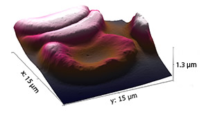
This year, the overall prize was won by this nice treatment of human red blood cells sent in by Akmaral.

|
||
Thanks to Christie for donating the blood!
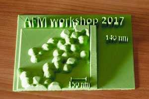
In addition, this year, we have a special prize for “outstanding image processing”, which goes to Tobias for this unusual image presentation: I can only show you a photo of the image, as he 3D-printed the AFM image of 90nm nanoparticles. Great one, Tobias!
3D printed image of Nanoparticles from Tobias Burger |
||
Congratulations to Akmaral and Tobias, your prizes and certificates will be with you soon!
Thanks to everyone who entered the competition this year. Hope to see you again!
- Details
- Hits: 6093
Atomic Force Microscopy (AFM) is a high resolution technique to measure the topography of samples. However, in order for such measurements to be accurate, the AFM must be calibrated, so that the results can be trusted. The commercial materials listed here are suitable for making such calibrations of AFM instruments.
This information on AFM standards is extracted from my forthcoming book "Atomic Force Microscopy".
Please get in touch if any information is inaccurate or you know of another standard or supplier.
See appendix B of Atomic Force Microscopy for calibration procedures.
X-Y Standards
These are standards to calibrate or check linearity in the X-Y axis in SPMs.
|
Source |
Standard |
|
VLSI standards |
many in µm range (silicon, 2D) 100 to 1000 nm (silicon, 1D) |
|
Ted Pella |
144 nm (aluminium on Silicon) 300 nm (titanium on silicon) |
|
MikroMasch |
3 and 10 µm, HOPG |
|
SPI Supplies |
300 or 700 nm (metal-coated silicon) |
|
Electron Microscopy Sciences |
300 or 700 nm (metal-coated silicon) |
|
Applied NanoStructures |
Various in micrometer range (metal-coated silicon). I personally tried use these standards. |
|
Bruker |
1, 2, 10, 15 µm (silicon) |
|
NT-MDT |
278 nm (aluminium on glass, 1D) 3 µm (silicon, 2D) |
|
Asylum Research |
10 and 20 µm pitch (metal on silicon) |
|
Nanosensors |
100, 200 or 300 nm (silicon) 4, 8 and 16 µm (silicon |
|
BudgetSensors |
500 nm, 5 and 10 µm - SiO2 on silicon. |
|
Team Nanotech |
Pitch and feature width standards |
|
Geller Micro |
Geller sell references and standards (including traceable ones), suitable for AFM as well as EM. |
Z standards
Here are standards to calibrate the z scale. Sometimes these can be the same ones as used for the x-y axis calibration, but often they are separate samples.
|
Source |
Z calibration standard |
|
VLSI standards |
various silicon and quartz |
|
MikroMasch |
Various in silicon, HOPG |
|
NTT AT |
Silicon monatomic steps (0.31 nm) |
|
Ted Pella |
20, 100 and 500nm (Silicon) |
|
Applied NanoStructures |
10nm, 1µm |
|
BudgetSensors |
10, 100 and 500 nm steps - SiO2 on silicon |
|
Veeco |
2, 100, or 200 nm (silicon) |
|
NT-MDT |
Various steps in silicon and atomic steps in Silicon (0.31 nm) |
|
Asylum Research |
200 nm (metal on silicon) |
|
Nanosensors |
8nm (silicon) |
|
Silios Technologies |
2, 5 and 10 nm (silicon) 1 nm "in development" |
Other standard materials include ultraflat samples - mica and HOPG, available from various suppliers, and quartz ultraflat sample from nanosensors.
Particle Standards
Particle samples are also useful both to calibrate the tip and as height references.
|
Supplier |
Particle sample |
|
Tedpella |
Gold colloids in 5, 15, or 15 nm diameter |
|
Edmund Optics |
Polystyrene nanospheres in a range from 20 to 900 nm |
|
Evident Technology |
Quantum dots ranging from 2.2 to 5.8 nm |
|
Electron Microscopy Sciences |
Colliodal gold in 0.8 to 25 nm diameter |
LFM Standards
Samples for calibrating LFM , with fixed angle slopes are:
|
Supplier |
LFM sample |
|
Mikromasch |
Triangles (silicon), top angle 70 ° Steps with sloped edges (silicon), slopes 54 ° |
|
Edmund Optics |
Ruled diffraction gratings, with various angles |
Phase References
Samples for calibrating phase are available from Asylum Research and EMS. Both are polymer samples with regions of different hardness.
Probe Shape Calibration Samples
These are samples you can image with the AFM in order to get an in situ measurement of the radius and shape of the probe tip.
|
Supplier |
Sample |
|
Aurora NanoDevices |
Tip check sample (100 nm z-scale). Nioprobe tipcheck sample ( 10 nm z scale) |
|
Mikromasch |
Porous aluminium |
|
NT-MDT |
Silicon spikes |
|
BudgetSensors |
Thin film on silicon wafer, with sharp pyramidal spikes. I have used this sample, and it can be used in contact or oscillating modes to characterise probe tip shape. |
Feel free to get in touch with any updates / corrections.
- Details
- Hits: 52874
Afmhelp.com has just been published, it does not have much content right now, but it's coming soon.
The website will launch towards the end of 2009, for more information see "About AFMHelp.com".
- Details
- Hits: 9002
This page has a list of corrections to the book "Atomic Force Microscopy". If you notice any more mistakes, please let me know here. That way I can correct them in the next edition!
Important Note: All these errors will be corrected in the upcoming paperback edition. If you know of any more, let me know!
Errors
- Page 30 - Equation 2.6: Verr is used in place of Zerr in the first term.
- Page 38 - The last paragraph erroneously refers to equations 2.5, 2.6 and 2.7, where it should be 2.7, 2.8 and 2.9, respectively.
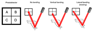
- page 53 - referring to the figure shown below:

In this figure, vertical bending is detected as "(A+B)-(C+D)", i.e. the difference of the top two and bottom two segments. On page 53 the book erroneously says "(A+B)-(C-D)".
- Page 56 - Figure 3.6 Should read: "B-intermittent contact oscillation (large)".
- Page 66 - Legend refers to colours in the image where there are none.
- Page 114 - Section 5.2.4: Three-dimensional views. Should read: "...special glasses to differentiate the left eye's and right eye's views...".
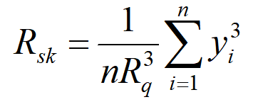
- Page 116 - Table 5.2. The Formula for skewness is incorect. The exponents should be 3, not 4. i.e., as shown below

- Page 164 - Misspelling of "fimbriae" as "fibriae".
Thanks very much to everyone who informed me of these errors!
- Details
- Hits: 15982
About AFMHelp.com
- What's this site about?
This site is designed to offer help with atomic force microscopy (AFM). AFM is an amazing and powerful technique for measuring images, and making other measurements of a wide range of samples. However, it can be rather daunting to use, especially for the beginner. On this website, as well as in the accompanying book we've collected a lot of information that explains how AFM works, and howto use AFM, and to process and analyse the images.
- What's AFM?
There's a lot of information about AFM all over this website, but for an overview, take a look at the AFM: Beginner's Guide page, and for frequently asked questions check out the AFM FAQ.
- Details
- Hits: 67283
Subcategories
Page 7 of 21


