
While many other procedures are important for full determination of the performance of an AFM instrument, the Z noise floor is often used as a simple parameter to quantify instrument performance, since it indicates the lower limit of the precision that can be reached in the z axis in that instrument, and is also simple to measure.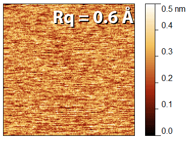
It can be essential to know the noise floor of the AFM instrument to assure that high resolution measurements are meaningful. This can be particularly important for measurements of very small features (i.e. < 5nm), and for high resolution force spectroscopy. Measuring the noise floor can also help in optimizing instrument setup and vibration isolation. It is important to know the noise floor when using only the z piezo in the z feedback loop, as well as the noise floor of the z calibration sensor if there is one in the instrument. In most instruments, the noise floor of the z calibration sensor will be much higher than that of the z piezo.
In order to get reproducible results, all scan parameters should be maintained the same when comparing two results. Some factors, such as the PID values vary greatly from instrument to instrument, so the specific values to use cannot be suggested here. In each case, standard values should be established such that a fair comparison can be made.
Note that the procedure below is adapted from general guidelines given in Appendix B, page 195 of Eaton and West “Atomic Force Microscopy”. For a outline of a procedure that’s generally applicable to any model of AFM, take a look at the procedure below. Click here to find a specific procedure for measuring the z noise floor on a TT-AFM from AFM workshop.
Measuring noise floor in the z piezo signal
a) Place a flat, clean sample in the instrument. Use a new probe.
b) Do a probe approach and scan a small image on the sample to verify cleanliness and optimize the PID parameters.
c) Set the instrument to make a zero size scan such that the probe does not move in the x and y axis. Some instruments do not seem to have the option to do this (I have found that the JPK Nanowizard software does not allow this). In this case, make the smallest size scan you are able to , such as 1nm, or even less if possible).
d) Measure an image without probe motion in x or y, i.e. an image with a scan size of 0 nm, at a 1 Hz scan rate. A 128 x 128 pixel image is adequate. The data from the z piezo voltage should be used. This may be labelled height, or topography. The z scale should be in nanometers.
e) It may be necessary to flatten the data before the measurement, e.g. by a 1st order horizontal line levelling routine.
f) Calculate the RMS roughness (Rq, see chapter 5) of the image, this value is the noise floor.
If you get some transient noise in the image, from e.g. a person talking, or slamming a door, you can repeat the image.
The achievable noise floor varies from one instrument to another, as well as depending on the noise in the environment, the measurement parameters, and the vibration isolation, but typically a sub-Ångström noise floor can be achieved. An example of type of image you should get is shown in the image above. it's important that you scan a small image before doing the "zero size" image, as the instrument must be in feedback for the noise floor to be measured.
All text and images copyright Peter Eaton 2014-2018
- Details
- Hits: 51846
A couple of new details about my book, Atomic Force Microscopy. Firstly, I just found a new (to me) review (published in German in Physik Magazine), including this great quote:
"Atomic Force Microscopy by Peter Eaton and Paul West is the manual that should accompany any AFM."
Prof. Othmar Marti, University of Ulm
Secondly, a new paperback edition of the book, was recently published. In addition to being approximately half the price of the hardback edition, this new edition has been updated and all (known) typos corrected, so this is the version to get if you can!
The paperback version can be found on amazon.com here.

- Details
- Hits: 6614
 |
| Bart showing his results |
Our atomic force microscopy training course for 2017 ran in April, between the 10th and the 13th. Once again, the course was a great success, and all the places were filled. In this post, I quote some of the the feedback we got from some of me of the attendees, as well as some of the images they produced. In this edition, the highlight (for me) was the talk from Prof. Bart Hoogenboom, from UCL.
Bart demonstrated some amazing results in AFM, and gave some real inspiration as to what AFM can achieve.
| Phase image of E. coli cells |
Once again, we had a good mix of students. They came from Wales, Portugal, Switzerland, the Netherlands, and Germany. We had PhD students, AFM technicians, lecturers, post-doctoral fellows and industrial researchers. It's always great to have such a wide range of opinions and nationalities!
As usual, we began with the basics of AFM, including instrumentation, modes, and fundamental concepts. Then the more fun parts, how to prepare samples, tips and tricks for running the instruments, and how to process and analyse the data.Most of the students prepared samples, and they all ran the instruments and processed and analysed image files. Based on the feed back, the students thought the course very worthwhile.
"I liked the course a lot. I think it's well-adapted to people with no AFM experience, and it seems it works well also for experienced users"
- Details
- Hits: 24015
My group recently published a paper in the journal Ultramicroscopy reporting on direct comparison we made between different techniques that can be used to characterise the size of nanoparticles.
There are a wide variety of technique available to make these kind of measurements nowadays, however, microscopy is often used, because it is a direct technique (some other techniques measure properties related to size), and because it’s also possible to measure shape at the same time. The size of nanoparticles is extremely important for their properties, and ideally a technique to measure nanoparticle size will have sub-nanometer resolution.
Apart from microscopy, light-scattering techniques are probably the most common techniques used. The method of dynamic light scattering, or DLS; is extremely popular and used in thousands of labs worldwide. A newer method based on laser light scattering, called nanoparticle tracking analysis, or NTA, is currently growing in popularity.
In our project, we prepared nine samples; these we made up of nanoparticles composed of three different, and commonly used materials, a metal, an oxide (silica), and a polymer. We examined each materials in two different sizes, and also tested the ability of each method to distinguish between different populations in mixed samples.
- Details
- Hits: 17999
I was recently asked what equipment is necessary to set up a new AFM lab, so here goes:
Materials necessary to set up a new AFM lab
Note: Many manufacturers include a lot of these items when you buy an instrument; check before ordering. I have only included estimated prices for items with high cost.
Mandatory Items
1. Calibration/certification product. Usually a silicon grid with repeating features. See extensive list of suppliers here:
SPM References and Standards
Note: This is the most expensive item, but absolutely necessary. The importance of calibration is discussed in my book (especially Appendices A and B). Take care of your calibration artifact once you have it.
Estimated cost: 300-1000 dollars, depending on model and supplier. Traceable standards will be more expensive.
2. Cantilevers / Probes. Of course these are necessary for all work. You typically get a few with a system, and can also beg samples from manufacturers, but you will need more, and soon! See extensive list of suppliers here:
Where to buy : SPM Probes
Estimated cost: 300 dollars for a box of 20
3. Anti-vibration solution. There are many different types of vibration-damping equipment, see chapter 2 of my book. They can usually be bought with instruments, but at additional cost. Suitable vibration / acoustic isolation stages for AFM instruments can cost from 2,000 to 10,000 dollars.
4. Tweezers. These are important for handling samples, and handling probes. I recommend two types, specific AFM probe-handling levers with specially shaped ends, and type 2A (flat, rounded ends, preferably non-magnetic), for handling samples and sample mounting discs.
I often buy from Ted Pella, see here for probe tweezers, and here for type 2A, but most microscopy suppliers carry these, or some equivalent. Note: on a budget, type 2A also can be used for probes, but I highly recommend that you keep a clean pair of tweezers, especially for handling probes.
5. Sample mounting discs. These are simply magnetic steel discs of about 10-15 mm diameter, and 1 mm thick. You can even make them yourself. Most microscopy suppliers sell them in tubes of 50-100. See here for the ones at Ted Pella.
6. Sample mounting adhesive tabs. To stick your sample onto the metal discs (above). See here for example at SPI. Alternatively, can be easily replaced with double sided sticky tape with few problems.
Optional Items
7. A source of very clean water. Some labs use milliQ water, and this is fine for most work, but you can also find ultra-pure bottled water, which I mostly use. See chapter 4 of my book.
8. A source of clean gas. Used for removing dust from samples. At a pinch you can use a “blower”, like this: Rocket Air Blaster.
9. Adhesive for when double-sided sticky tape is not enough: 2 part epoxy is the gold standard, superglue (cyanoacrylate) can also be used, but not for work in liquids.
10. Solvents for cleaning, etc.
11. Optical microscope and / or magnifier. Usually AFMs have an integrated optical scope, that can be used to obtain optical images of the sample. Depending on your application, and how good the attached scope is, you may want a separate optical microscope to view samples before putting them in the microscope and possibly to record good optical images. This can help greatly with sample preparation. It is also VERY useful to have a magnifier or small microscope to help with probe seating, i.e. to make sure your probe chip still has a cantilever and that you have placed it in the probe holder of the AFM correctly.
12. Other susbstrates. Depending n the kind of work you need to do, you will want substrates to deposit your samples on. These might be optical glass slides, coverslips, mica, or HOPG. flat silicon samples can also be useful. Most AFMs work with 1cm diameter samples or smaller.
Instrument Building / Repair / Diagnostics
For this, you’ll also want many small tools, including Allen (hex) keys, screwdrivers, etc. Glue, including superglue. Multimeter. Good soldering iron and solder, preferably silver solder with a flux core.
Room Requirements
For the room you are going to put the AFM in, there are not many real “must-haves”. But it’s recommended you use a small lab, with little foot traffic, or at least one where the people can be expected to keep quiet. Basement labs are preferred to upper stories. These are all due to vibration and acoustic noise issues. It’s useful to have air-conditioning, especially if you expect to have large temperature variations during the day. But you must be able to turn this off in case it interferes with high-resolution work.
As always, suggestions and additions to this are welcome - go HERE for the contact form.
Copyright Peter Eaton 2012-2018
- Details
- Hits: 30218
Subcategories
Page 6 of 21